Iiyama, meet Xilinx
Recycle old electronics for hacks
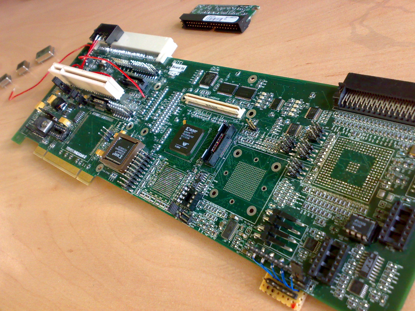
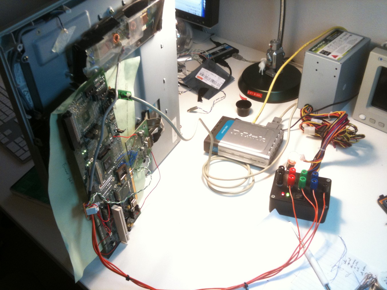
I bought a random PCI card from WeirdStuff surplus warehouse on a Sunday morning. I think I had just had some pancakes, probably with strawberries, but that’s not important right now. Anyway, this was an Intel-made full-length PCI card that looked like a prototype for a h.100 weird telephony bus somethingorother. It has a small serial number, is chock full of testpoints and analyser connections, a PCI-PCI bridge etc. The reason I bought it, though, was that it carried a Xilinx Virtex-E FPGA so could be reprogrammed to Do Stuff.
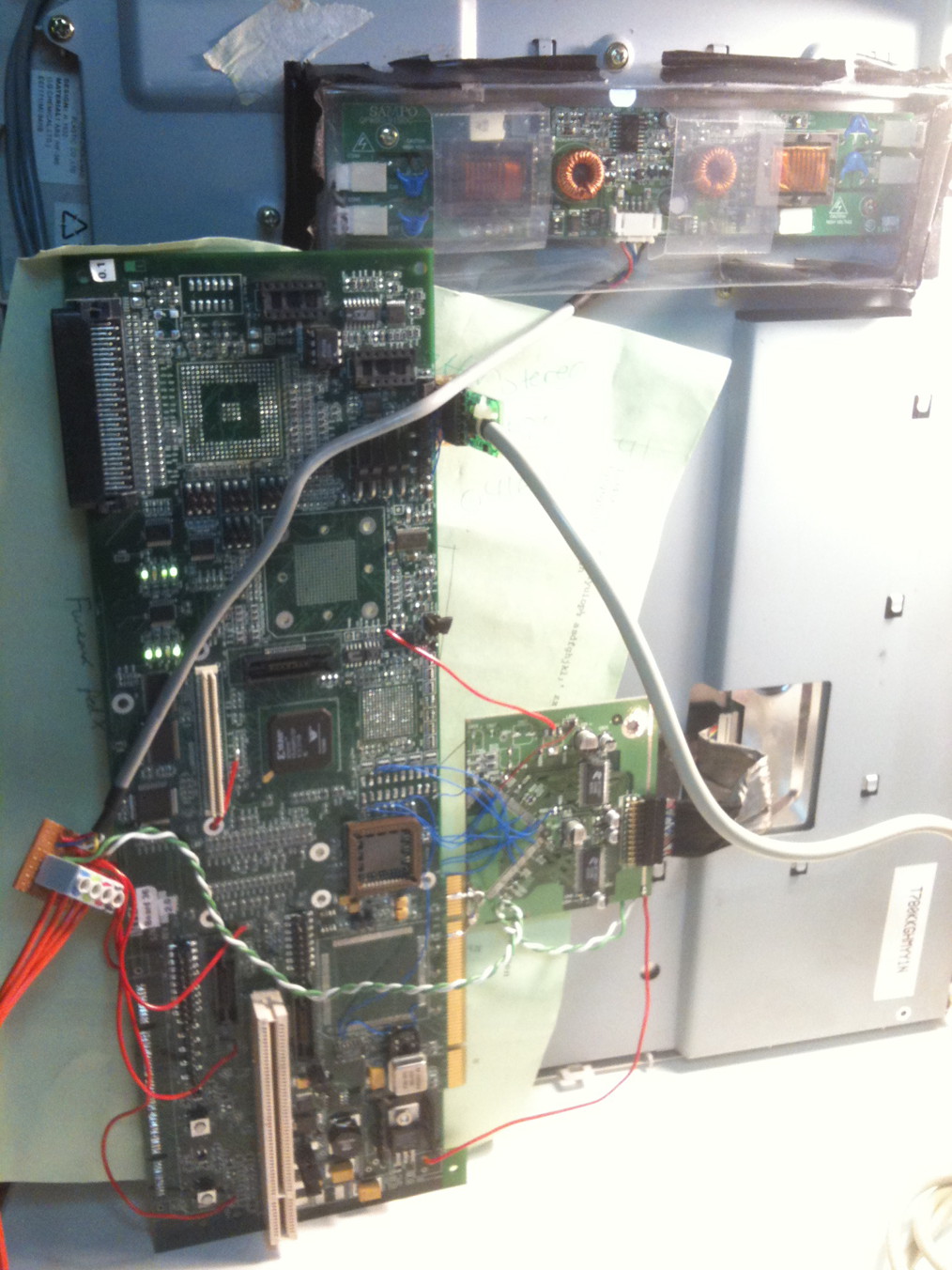
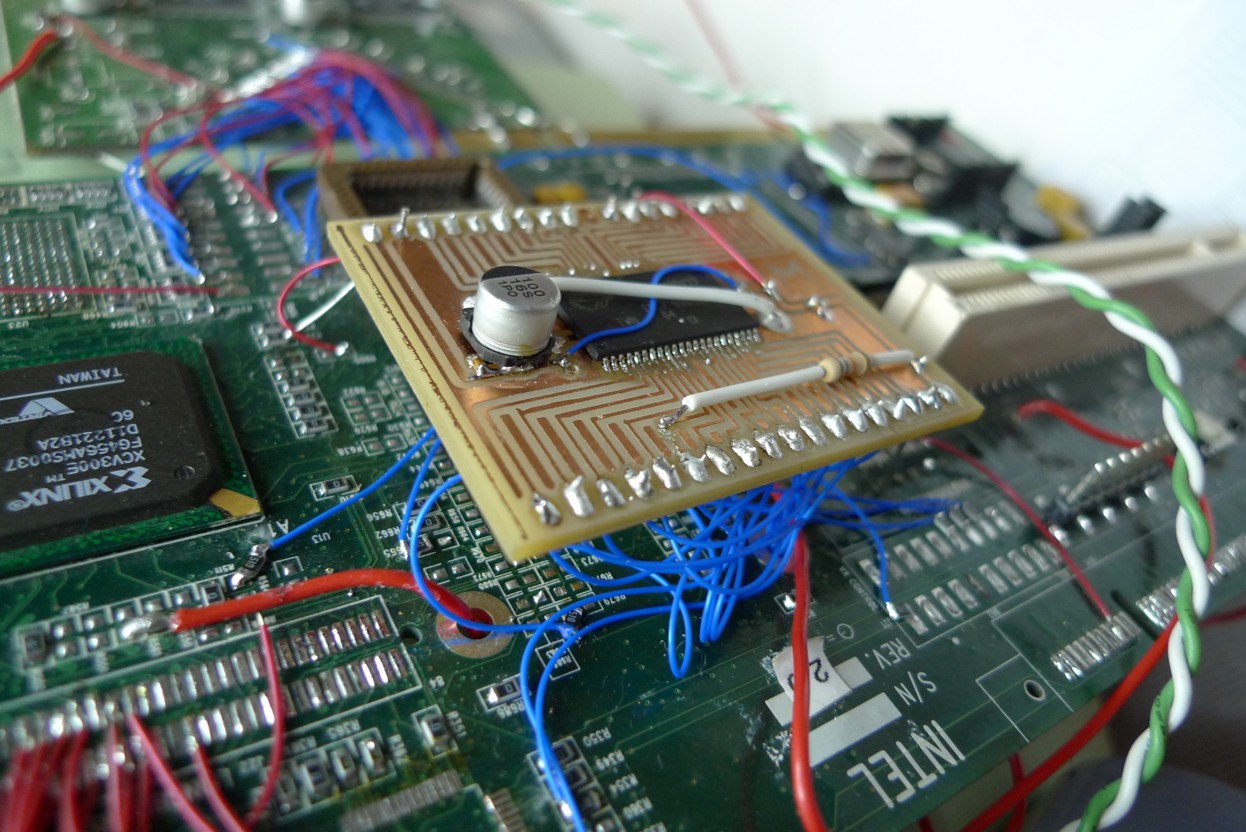
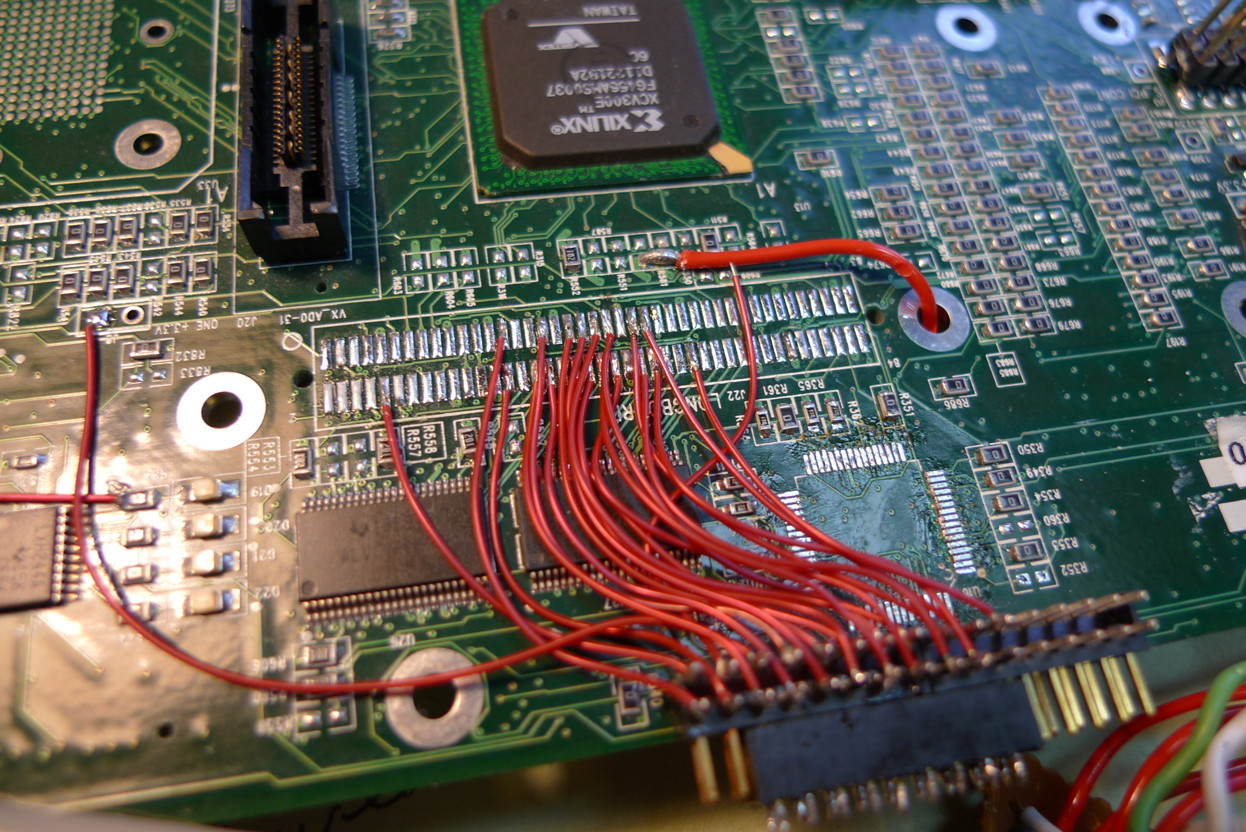
I also got a broken Iiyama 17” monitor from work. This has a 1280x1024 panel driven as two 24bit pixels in parallel over two separate LVDS links. I desoldered the unnecessary chips from the PCI card to free up I/O pins (the PCI-PCI bridge and h.100 controller), then reverse-engineered parts of the PCB to work out which FPGA pins went where. (I used a demo of MitouJTAG and then when I couldn’t take that anymore, my own autogenerated verilog-plus-ANSI-graphics frontend, TBR). With this list of connections, I have a general-purpose FPGA dev board! ;-) It’s an XCV300E Virtex part, so not too crap for a $4 piece of junk.
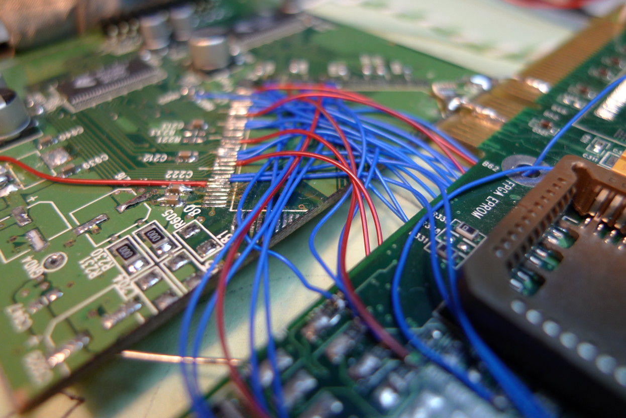
The monitor panel I used was working fine, but its 8051 microcontroller on the driver board was unhappy. I dremelled the LVDS section of the board out, leaving the high-speed serial connections intact but giving me access to the slower RGB parallel data input to the LVDS serialisers. Two pixels at a time plus syncs/clock is 51 little TQFP208 pads to solder onto.
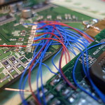
[Ed: The signals from FPGA to LVDS board are series-terminated at source using tombstone-mounted (IIRC) 68 ohm resistors (I didn’t promise it was pretty); the poor grounding, relatively high speed and relatively long wires would detract from signal quality and we don’t want no stinking ringing at high speed!]
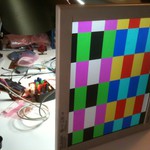
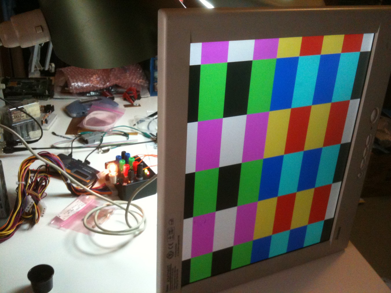
Shown below is a basic test card; it got incrementally more colourful as I added more of the RGB data :-)
GBA video input and scaler
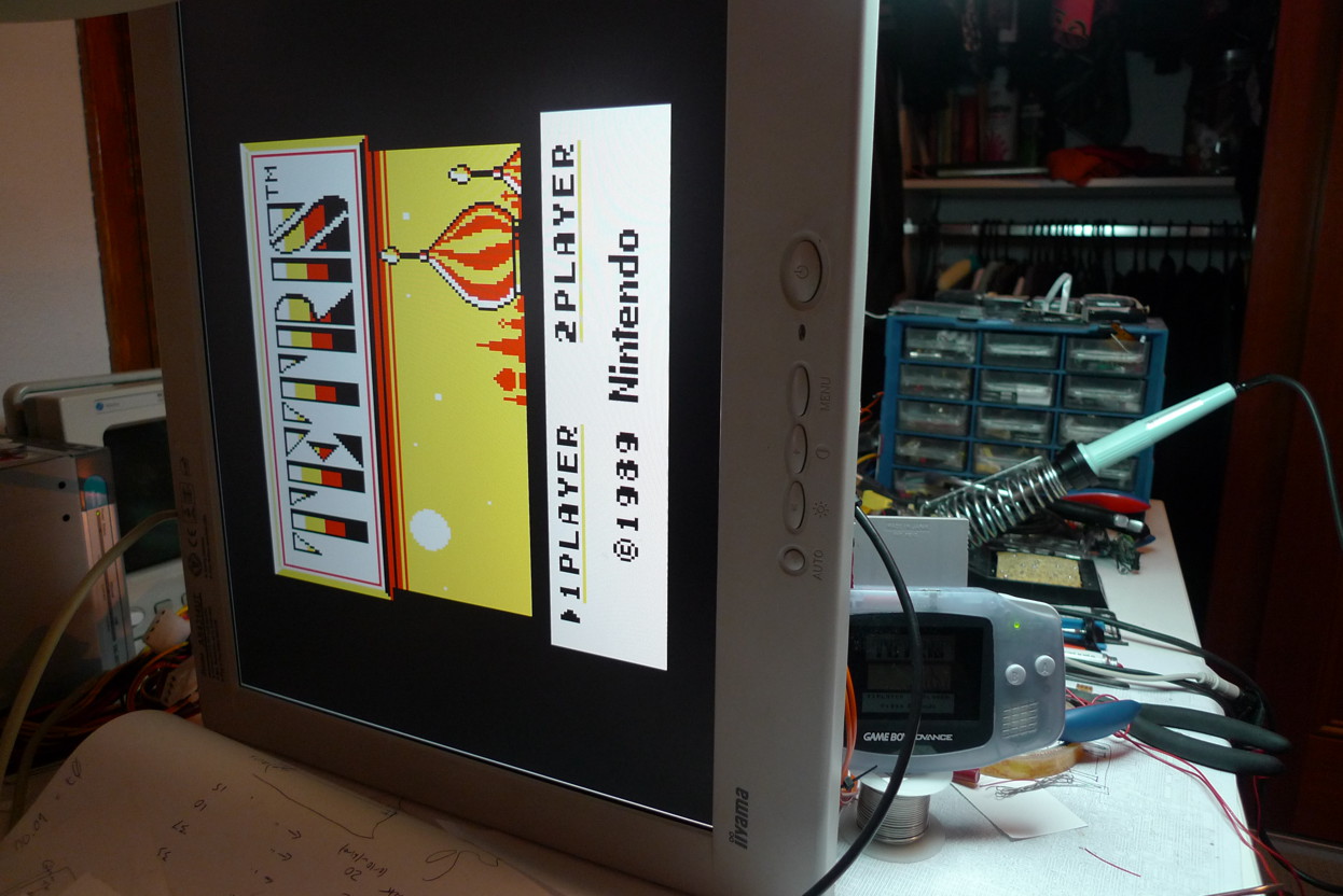
With the LCD-driving side of things working, I added an input port to connect my old Gameboy Advance’s video circuitry to the FPGA.
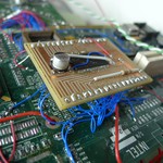
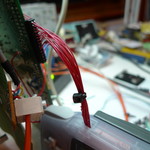
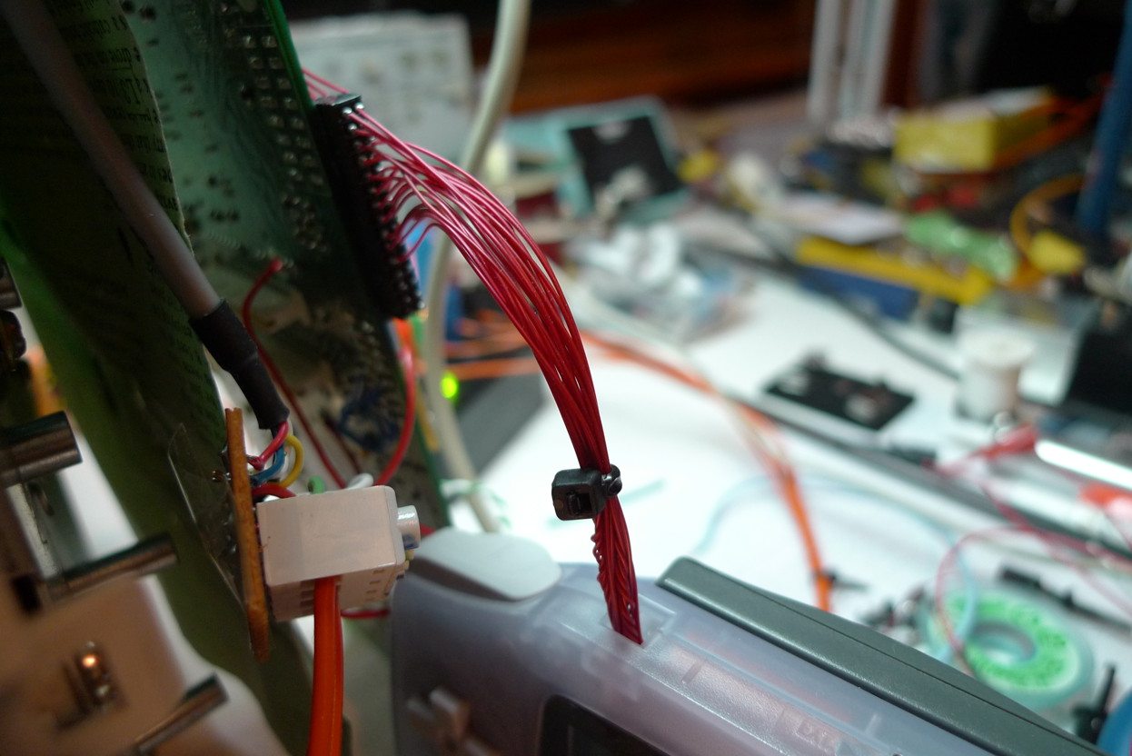
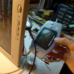
I tapped into the GBA’s LCD signals (RGB of 5 bits each, VSYNC and pixel CLK), which are brought out to little red wires (see pic). The GBA’s LCD remains in place, and is functional. These are sampled by the FPGA on the GBA-generated pixel clock (~2.4MHz), buffered (into a blockram, BRAM, on the FPGA) and written into 512KB of 10ns SRAM which was also added with a little daughterboard (see pic). The RAM’s 8 bits wide, so provides 50MB/s of read bandwidth (I’m using a 50MHz sysclock).
The FPGA design implements:
- WishBone interconnect (8 bits wide, for 3 masters: LCD controller, debug cell, GBA DMA)
- SRAM controller, interfacing the external RAM with WB (ish; it bends the WB rules a little to allow faster burst reads/writes).
- Debug cell (UART/basic read-write/IO over WB)
- GBA-to-FIFO-to-WB-to-SRAM video input DMA master
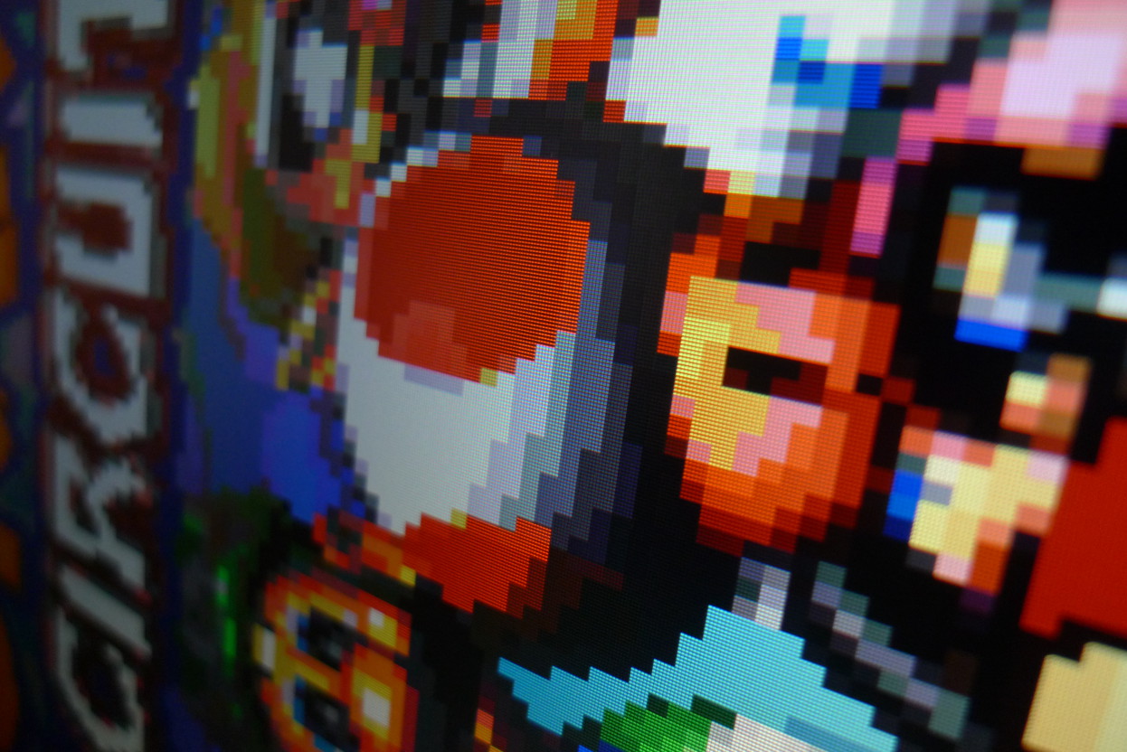
- SRAM-to-LCD video scaler, upscaling 240x160 to 1200x960 and centring that on 1280x1024 LCD.
The LCD runs at 55ish Hz refresh (as the pixel clock’s 50MHz due to having a 50MHz oscillator lying around; 60Hz needs ~54MHz). The LCD image is scaled x5 in X and x6 in Y; it doesn’t do any snazzy filtering partly because I’m lazy but also because I wanted big chunky retro pixels. Since the same line will be displayed on the TFT six times, the pixel data is read over WishBone from RAM but buffered in a BRAM (0.5KB); bus utilisation is kept to the minimum. (This is actually double-buffered; as one GBA line is displayed the six times, the next line is being fetched from RAM into a second BRAM.)
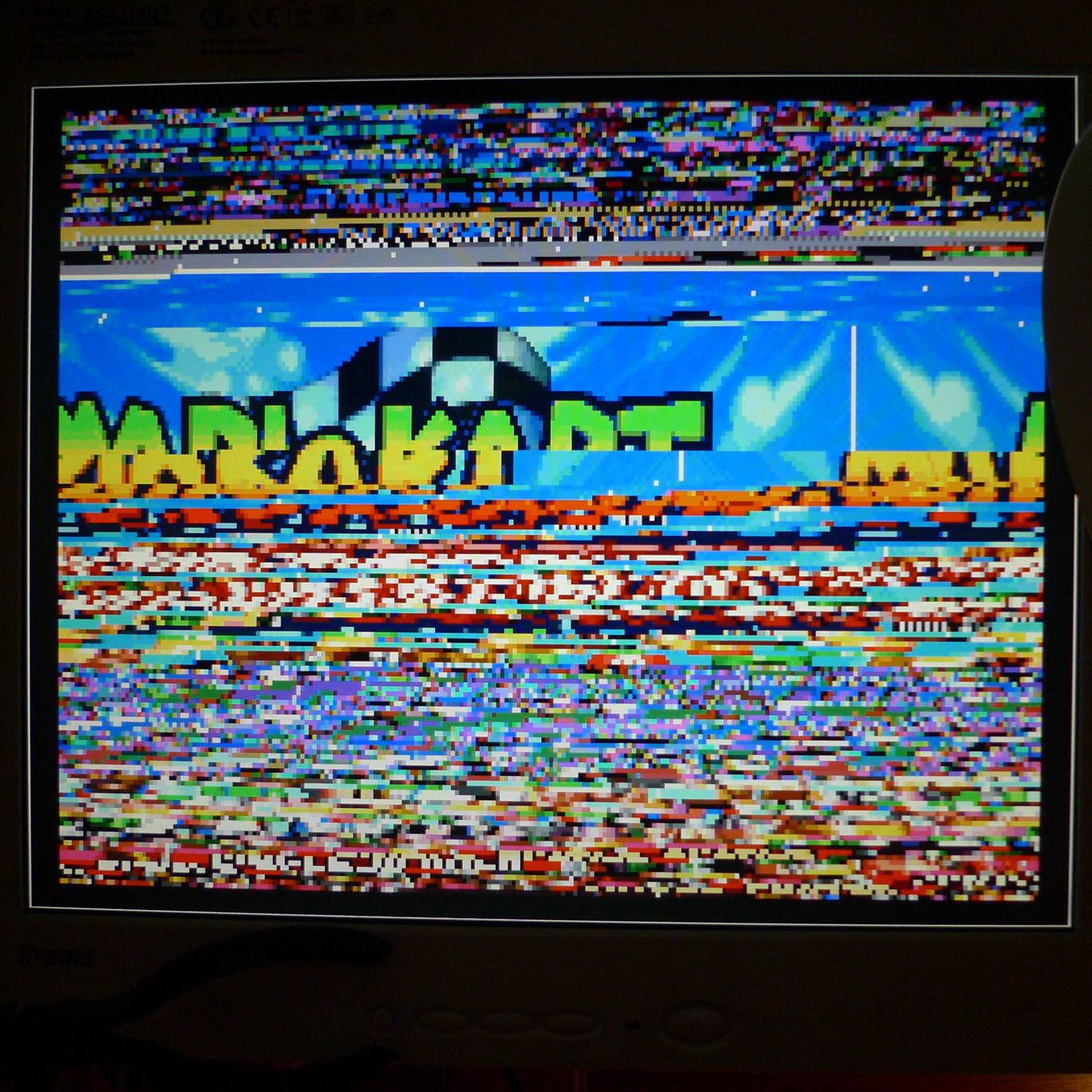
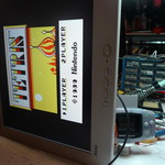
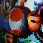
It’s surprisingly tear-free (in both respects) without double-buffering the actual frames themselves! (The input rate is 60Hz, output is asynchronous and ~55Hz.) Pictured are some of the initial tests. The cat image was downloaded over a noisy/unreliable serial link (see the corrupt pixels!) and, well, you can see my first attempt at the GBA video DMA. Once I’d started not doing it wrong, it was OK.
I’d like to make this into a cocktail table-style crappy ‘arcade’ machine; future plans hardware-wise are:
- Retrocomputing with a soft CPU core
- Add SNES controller (really for the shoulder buttons, to mimic the GBA)
- Experiment with basic sprite engine, with soft core on the FPGA to make my own (possibly awful, but that’s… the… magic of it) games machine.
I use the wrtag box to program the FPGA’s bitstream. All in all, on top of the surplus PCI card I spent about $5 – on the SRAM, the only extra part I purchased; everything else I had lying around. I learned a lot about signal integrity/termination and debugging the analogue side of high-speed digital circuits. I would not advocate copying this construction method (airwires, airwires, airwires); it’s tongue-in-cheek engineering, trying to really see what’s possible performance-wise with random PCBs, hand-made airwire construction, etc. Turns out, quite a lot! :-)
Built Jan-May 2011
Images
-
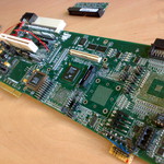
- Almost-original FPGA board (ICs removed)
-
- Driving LVDS serialiser inputs via pads
-
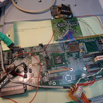
- Overall view

-
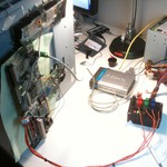
- Experimental setup
-
- Display works
-
- SRAM carrier board

-
- System, SRAM carrier, GBA

-
- Parallel video input
-
- LCD wires exiting GBA case

-
- Cat closeup
-
- Oops...
-

- It's alive!
-
- Display mirrored
-
- GBC mode
-
- Nice chunky pixels!
Video of initial testing
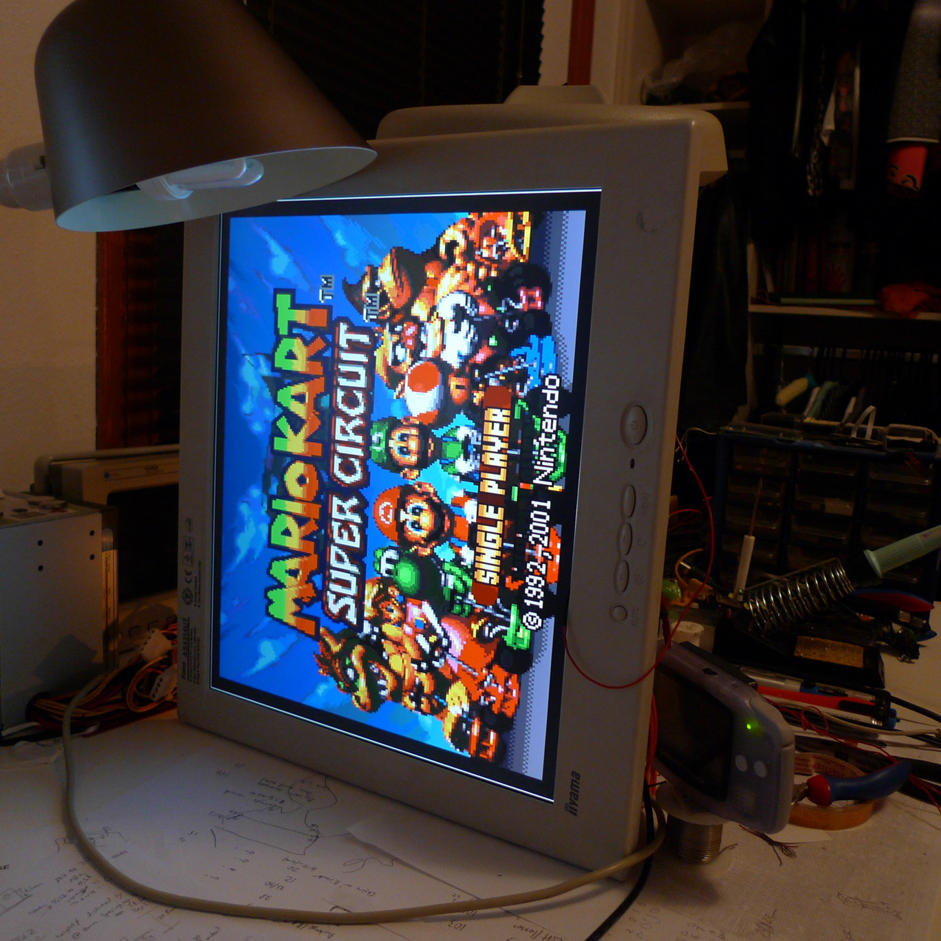
[ AKA “I’m a bit crap at Mario Kart” :) ]
Edit: The screen is on its side as that way it balances nicely against the desklamp with wires/PCB hanging safely. It will work any way up. :)